Fills not including pads
HI there! I hate to be a pain, but I just recently picked up Kicad (Eagle was my first pcb design program). So far everything with Kicad has been great! However, I have recently run into a perplexing situation. I've created 2 ground copper fills, one on the back layer and one on the front. However, the fills do not visibly connect with the pads, no thermals, nothing, no matter what settings i seem to tick in the fill properties. I've made sure that the fills are connecting the ground nets, but they still seem to not actually connect to any pads at all. I've even tried running some vias from the grounds pads to the fills, and they seem to vanish from the final gerber files.
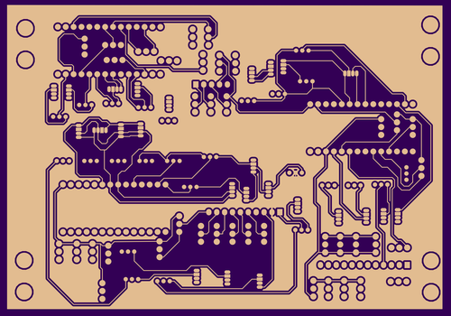
Here's one side of the board, according to osh park, for further reference:
https:/
btw, I'm on windows 7, running kicad ver 4.0.1-stable
any ideas?
thanks again for your time, I do really appreciate ya'll and the dev'ing of this software!
Question information
- Language:
- English Edit question
- Status:
- Answered
- For:
- KiCad Edit question
- Assignee:
- No assignee Edit question
- Last query:
- Last reply:

Can you help with this problem?
Provide an answer of your own, or ask McAleister Billiams for more information if necessary.